400-9920-618
In recent years, RFID technology and products have been widely used in various industries. What is the manufacturing process of RFID chips?
It Is said that the chip manufacturing process just like building a house with Lego. First, the wafer is used as the foundation, and after the chip manufacturing process is stacked up layer by layer, the necessary IC chips can be produced. But the most important part is always ignored. If there is no designer, no matter how superb the skills are, it is useless. Just like a piece of clothing needs a tailor, but if there is no clothing designer to design good-looking clothes, how can a tailor make good-looking clothes.
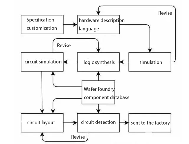
So what is the process of chip design? here a flow chart can show it
After understanding the chip design process, let's take a look at the foundation "wafer".
Wafer is the basis for manufacturing various computer chips. We can compare chip manufacturing to building a house with Lego blocks, and by stacking layers one after another, we can complete the shape we want (that is, all kinds of chips).
In solid materials, there is a special crystal structure - monocrystalline (Monocrystalline). It has the property that atoms are packed close together, one behind the other, to form a flat atomic surface. Therefore, using a single crystal to make a wafer can meet the above requirements. However, how to produce such a material mainly involves two steps, namely purification and crystal pulling, after which such a material can be completed.
Next, let's go into the key points and see how IC chips are manufactured.
First of all, let's first understand what is an IC chip? IC, the full name of Integrated Circuit, can be known from its name that it combines the designed circuits in a stacked manner. By this method, we can reduce the area required to connect the circuits.
How is it manufactured? Just imagine, if we want to make fine drawings with paint spray cans, we need to cut out the cover board of the graphics and cover them on the paper. Then spray the paint evenly on the paper, and after the paint dries, remove the mask. After repeating this step continuously, neat and complex graphics can be completed. Manufacturing ICs is done in a similar way, layer by layer by masking.
When making an IC, it can be easily divided into the above four steps. Although there are differences in manufacturing steps and materials used in actual manufacturing, they generally adopt similar principles.
1. Coating photoresist
Put the photoresist material on the wafer first, and hit the light beam on the unnecessary part through the mask to destroy the photoresist material structure. Next, the damaged material is washed away with chemicals.
2. Etching technology
The silicon wafer, which is not protected by photoresist, is etched with an ion beam.
3. Photoresist removal
Use the photoresist remover to dissolve the remaining photoresist, thus completing the process once.
In the end, many IC chips will be completed on a whole wafer, and then the completed square IC chips can be cut out and sent to a packaging factory for packaging.
After reading the above manufacturing method, maybe you will ask what is the package?
After a long process, from design to manufacture, an IC chip is finally obtained. But since a chip is quite small and thin, it will be easily scratched and damaged if it is not protected externally. In addition, because the size of the chip is small, it will not be easy to manually place it on the circuit board without a larger-sized casing, so it needs to be packaged.
There are two common packages at present, one is the DIP package that is black and looks like a centipede, which is common in electric toys, and the other is the BGA package that is common when buying boxed CPUs.
7 * 24-hour service hotline
Room 702, Building 5, Gonglian Urban Intelligence Valley, No. 58, Ping'an Road, Guanlan Street,Longhua District, Shenzhen,China,518110
E-mail: info@hhw9.com